Since 2020 CKTECH has cooperated comprehensively with NXP. Based on NXP ARM and SoC chip CKTECH has independently developed 5G RAN platform including 5G RAN L1 physical layer and L2/L3 high-level protocol stack software. CKTECH devotes to build a low-power, customizable 5G RAN ecosystem to derive a variety form of 5G Base Station solutions based on the self-developed 5G RAN technology platform.
The 5G RAN platform has the advantages and characteristics of higher integration, smaller volume, lower power consumption and higher cos-effective. Based on the platform CKTECH can provide various type of 5G RAN products such as distributed and integrated 5G Base Station, 5G femto Base Station. CKTECH is able to develop 5G NR protocol stack independently and can provide customized 5G Base Station solutions according to customer’s requirements to meet various 5G application scenarios for families, SOHO, enterprises / industrial parks and telecom operators.
1. Advantages of 5G RAN platform
a) The power consumption of 5G RAN platform is lower and cost-effective, which can effectively reduce CAPEX and OPEX.
b) The 5G RAN platform supports hardware acceleration for the processes of air-interface integrity protection, PDCP encryption and decryption, IPSec functions, etc. and can further reduce the system power consumption of the 5G RAN while ensuring its performance.
c) The baseband core physical layer is all implemented by software code, which is open. Therefore, it can be customized according to customer’s requirements, and makes it easy to add and realize new customized functions.
2. Introduction of NXP ARM chip
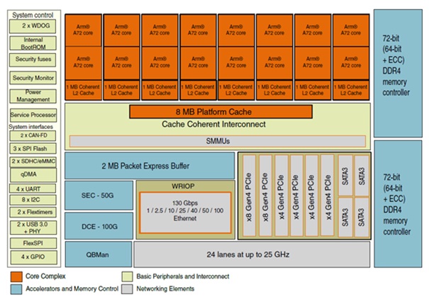
The advanced sixteen-core 64-bit ARM processor, LX2160 is ideal for applications such as 5G packet processing, network function virtualization (NFV), white-box switching, high-processing industrial computers, machine learning and smart Network Interface Cards. The high level of integration delivers significant performance benefits such as 100GbE, hardware L2 switching, DPAA2 with 100Gbps decompression/compression and 50Gbps SEC and multiple PCIe Gen3.0 and SATA controllers.
For Edge Computing, this processor offers outstanding computing performance with a powerful packet offload and Ethernet controllers. You can have high-end and high-speed communications in one device, with low-speed peripherals such as sensors and the computing power to process and act upon all received information.

The architecture of LX2160 chip
3. Introduction of NXP SoC chip
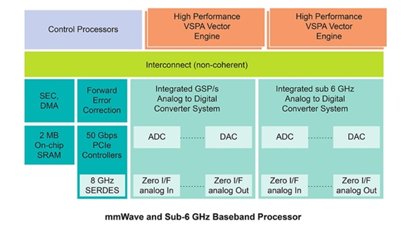
The LA12XX is a high-performance vector VSPA DSP with built-in bit-level accelerators (including LDPC and Polar codecs). The LA12XX has multiple e200 master cores and multiple high-performance vector VSPAs. A single LA12XX can enables complete physical layer processing for a 4-antenna 100MHz bandwidth NR cell. The LA12XX supports up to 13Gbps coding and 9Gbps decoding capacity, which is fully satisfied with the peak throughput processing capability of a 4-antenna 100MHz cell.

The architecture of LA12XX SoC chip


+86-10-62060415


